


Best viewed using:
Internet Explorer
or
Mozilla Firefox


N8105 LED Power Distribution Jr. Layout
Figure 1 shows the front and back view of the N8105. Layout details are noted by a red circled area and corresponding number. The corresponding numbers are described below:
-
Shows the 20ma current source chip on the top or front side of the board.
-
Indicates the +DC input voltage connection point.
-
Indicates the –DC input voltage (or DC ground) connection.
-
Marks the placement of the top-side LED solder pad pairs. Note that each pad pair has one oval or rounded pad and one rectangular pad. The rounded pad is the anode or + LED connection point, the rectangular pad is the cathode or – LED connection point. The top side allows for up to 4 LEDs, which would be wired as a series connected group (depending on available supply voltage).
-
This is a cathode grounding point (-DC) that can be bridged with a drop of solder to complete the circuit. If only 1 LED is to be wired in the group, then LED1’s cathode should be solder-bridged (to complete the circuit). If there will be 2 LEDs in series, then solder the grounding bridge for the cathode of LED2 (and do not solder LED1’s cathode bridge). If 3 are needed, then bridge the cathode of LED3. LED4’s cathode is grounded by default. If less than 4 LEDs in the group are used, LED4’s cathode won’t be connect anyway. You’ll notice that the cathode of LED A and the anode of LED B are connected (also LED B to LED C, and LED C to LED D). This allows the user just make wire hookups from the LEDs to the board without having to connect wire to wires for series connections.
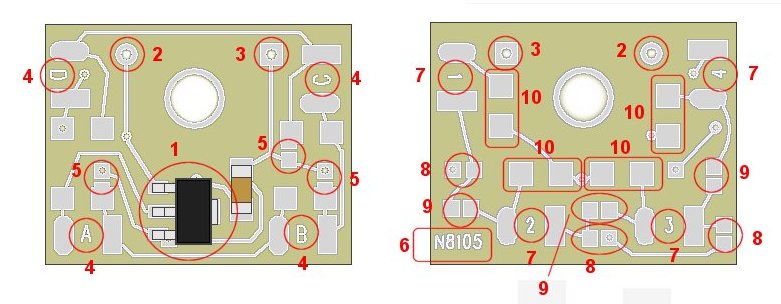
Figure 1
-
Shows the board part number. This appears only on the back or rear side of the board.
-
Marks the placement of the bottom-side LED solder pad pairs. Again, each pad pair has one oval or rounded pad and one rectangular pad. The rounded pad is the anode or + LED connection point, the rectangular pad is the cathode or – LED connection point. The bottom side of the board provides connection for up to 4 additional LEDs, which can be connected as one or more series groups, individually (parallel) wired LEDs, or a combination of both.
-
Show the solder bridge points that connect an individual LED's cathode to –DC (ground). These points are used when an individual LED is wired with its own resistor (parallel configuration) or, to end (ground) the last cathode in a series group. LED 4's cathode is grounded (connected to –DC) by default.
Very important: Never solder both 8 and 9 bridge points between any two LEDs - ever! The will cause a short to your power source and will damage the Distribution Board.
-
Notes the solder bridge points to connect LED cathodes and anodes to create series groups. Example: LED 1 cathode has a connection to a bridge point that, if soldered, connects it to the anode of LED 2. There is another bridge point for the cathode of LED 2 and the anode of LED 3, and another for the cathode of LED 3 and the anode of LED 4. If all three of bridge point 9's were soldered, the bottom of the board would be configured for a series group containing 4 LEDs.
-
Shown the solder pads for installing current limiting resistors for the 4 different LEDs on the bottom side of the board. Only 1 resistor would be used for any series group of LEDs.
The flexibility of the bottom side of this board allows for many different combinations of LED wiring schemes. This will give the hobbyist many options when lighting a project. Examples can be found by clicking here.
© 2011 Ngineering